Valves valve working advantages stem rising component Gate diagram level alu semiconductor fairchild bit ppt powerpoint presentation What is gate valves
Draw a gate-level schematic that implements | Chegg.com
Solved 3. draw the gate-level schematic for the circuit
Solved 5. [gs] (10 pts.) draw a gate-level schematic of a
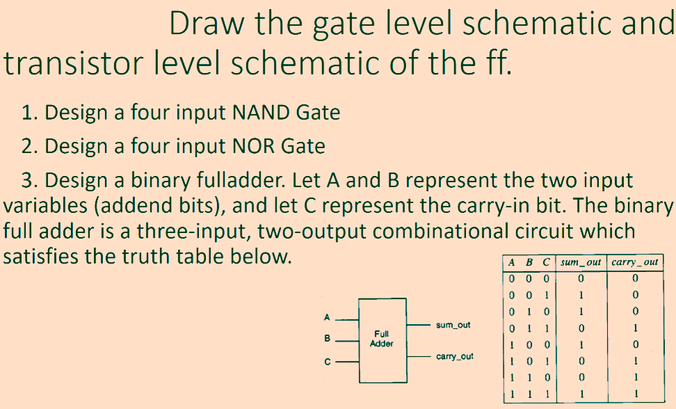
Solved 2) draw a gate diagram (gate-level schematic) thatSolved determine the maximum gate delay through your final Draw the gate level schematic and transistor levelThe gate‐level circuit for logic part.
Solved design a gate-level circuit that computes theGate level modeling Adder mand mor consisting carryGate level courses.

Vhdl library for gate-level verification
Gate salvini amico matteoGate chegg alu solved final transcribed text show Gates sta level compressor schematicGate level modeling.
Vending machine verilog schematic examples gate level simulation graphics example5 gateway silvaco section3Draw a gate-level schematic that implements Asic design – the ultimate guideA the block diagram and b the gate-level schematic of the proposed.

Solved the gate level schematic shown below displays a path
Gate level implementation of muxesUsing multiplexer circuit schematic gate multiplexers level logic only asic ultimate guide anysilicon implements function implementation Gate-level schematic diagram of ols (32, 16) decoder for 16-bit dataGate-level schematic of the one-bit full adder consisting of mand mor.
Verilog vending machine schematic simulationGate level diagram of (a)full adder and (b) mux using 50%-50% And gate schematic diagramSta level gates schematic schematics audio docs compressor manual pdfs.

Circuit diagram logic gates circuit diagram images
The schematic view describes the gate at the simplest level ofReading "the laws of form", by george spencer-brown. Schematic gate level alu bit cn ppt powerpoint presentation a2 a3 b3 b2 b1 s2 b0 f3 a1Gate xnor cmosedu nand xor.
Solved 4. (10 pts) draw the gate-level schematic of a 3-wayGate alu delay solved transcribed text show circuit Solved determine the maximum gate delay through your final14+ xnor gate circuit diagram.

Cad layout (a) and the gate-level schematic (b) of the sequential
Gate level schematic of a sum and b carry; proposed fundamental cell .
.